- Programmers Reference
- Bringup Sequence
-
Bring up sequence.
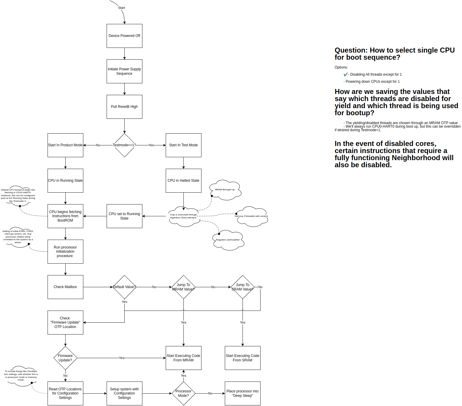
First boot on the tester.
- TestMode pin is held high. CPU is halted (in reset mode?)
- POR is toggled.
- OSC_CLK_OUT is measured, the PPM difference from expected frequency is calculated.
- Osc TRIM Parameters are calculated. (Index in Trim table?)
- Part is speed graded.
- Osc TRIM parameters and speed grade is written to OTP
Second Boot.
- TestMode is held low.
- CPU Starts executing bootrom code.
- OTP is read(Trim Param, Speed grade, ROM Update).
- If ROM Update bit set, jump to updated firmware in MRAM.
- Trim Ring Oscillator.
- Program RO-CLK Div for highest clk freq supported by device speed grade.
- Calculate Clk Div for Periph and MRAM.
- Program Periph clkdiv and mram clkdiv.
- Read CHIPMODE.bootloader register to determine location of application code (TCM,MRAM(default))
- Jump to application code.
Program Mode
- Bring MRAM out of deep sleep.
- Load MRAM/TCM with the application code
- Set CHIPMODE.bootloader register.
Application Code
- If MRAM is in deep sleep mode it needs to be brought out of sleep.
- Write to
system_registers.PowerDomainReq.mram_dsleep_en to bring MRAM out of deep sleep.
- Use
system_registers.Mailbox0.mbox0 and system_registers.Mailbox1.mbox1 for communication from CPU to host chip and vice versa.