Erbium CPU Subsystem: High Level Architecture and Programming Model
The CPU subsystem enables the Erbium platform to operate as an Edge AI device. In this mode, the CPU subsystem is the primary transaction initiator on the AXI4 interconnect to which it is connected.
The main CPU subsystem components are:
- ET‑Neighborhood with 8 ET‑Minion cores
- 32KB L1 I‑Cache data SRAM
- Platform-Level Interrupt Controller (PLIC)
- CPU Registers
- Synchronization primitives: Fast Local Barriers, Fast Credit Counters
- CLINT logic
Table of Contents
- 1. CPU Subsystem hierarchy
- 1.1 ET-Minion
- 1.2 ET-Neighborhood
- 1.3 CPU Subsystem
- 2. Programming Model
- 2.1 ET System Registers (ESR)
- 2.2 Register File changes
- 2.3 ET-Minion SIMD
- 2.4 Floating‑Point Denormal Handling
- 2.5 Performance Monitoring Unit (PMU)
- 2.6 Privileged Architecture Deviations
- 2.7 Exceptions and Interrupts
- 2.8 Synchronization primitives
- 2.9 Core Local Interrupt (CLINT)
- 3 ISA changes (Erbium)
- 4. Erbium Memory
- 4.1 Memory Map
- 4.2 Physical Memory Attributes
- 4.3 Physical Memory Protection (PMP)
1. CPU Subsystem hierarchy
The hierarchy builds from the smallest unit upward starting from the ET-Minions.
1.1 ET-Minion
At the lowest level of the hierarchy there are the ET-Minion cores. Each ET-Minion core is a dual-threaded, in-order, single-issue, RISC-V core extended with a proprietary 8-lane SIMD extension. Specifically, the ET-Minion core implements the following RISC-V architecture:
| Base | Version | Comments |
|---|---|---|
| RV64I | 2.1 |
| Extension | Version | Comments |
|---|---|---|
| M | 2.0 | |
| F | 2.2 | Not fully compliant; see Programming Model |
| C | 2.0 | |
| Zicsr | 2.0 | |
| Zifencei | 2.0 |
| Module | Version | Comments |
|---|---|---|
| Machine ISA | 1.11 | Not fully compliant; see Programming Model |
| Supervisor ISA | 1.11 | Not fully compliant; see Programming Model |
Each ET-Minion core has its own 4KB private L1 Data Cache (that can also act as a scratchpad) but does not have a private Instruction Cache. The vector unit supports a custom ET-Minion SIMD extension that allows operating on eight floating point values in the same cycle. The vector unit supports transcendental instructions and tensor instructions that accelerate machine learning applications.
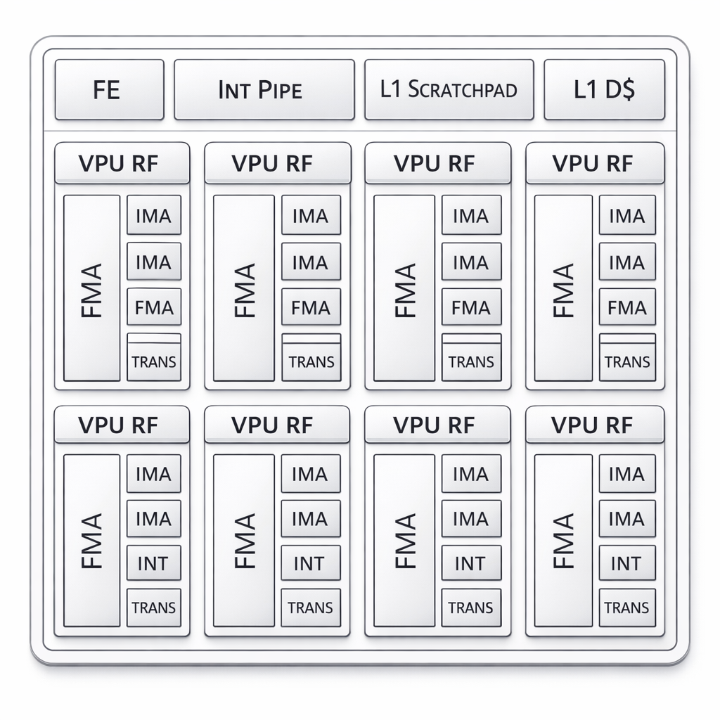
The ET-Minion is composed of a front-end (FE) unit for fetching instructions from an external, shared, Instruction Cache. Instructions are then fed to the Decoder unit (part of the FE) that will ship them either to the Integer/Dcache pipeline or to the Vector unit pipeline.
The Vector Processing Unit (VPU) is composed of eight identical lanes. Lanes always operate completely synchronously, so to the final programmer the VPU appears as a single entity that performs 8 operations per cycle. Each VPU Lane contains:
- A register file holding thirty-two 32b-wide registers. When viewed together, the eight lanes present to the programmer as a unified register file containing thirty-two 256b-wide registers.
- A Fused Multiply‑Accumulate (FMA) unit capable of performing one 32b or two 16b floating point multiply-add operations
- A pair of Integer Multiply‑Accumulate (IMA) units each capable of performing four 8b integer multiply-accumulate operations
- An Integer (Int) unit capable of performing 32b integer and logical operations
- A Transcendental (Trans) unit capable of performing 32b floating point transcendental instructions (
sin,exp,log,rcp,rsqrt)
1.2 ET-Neighborhood
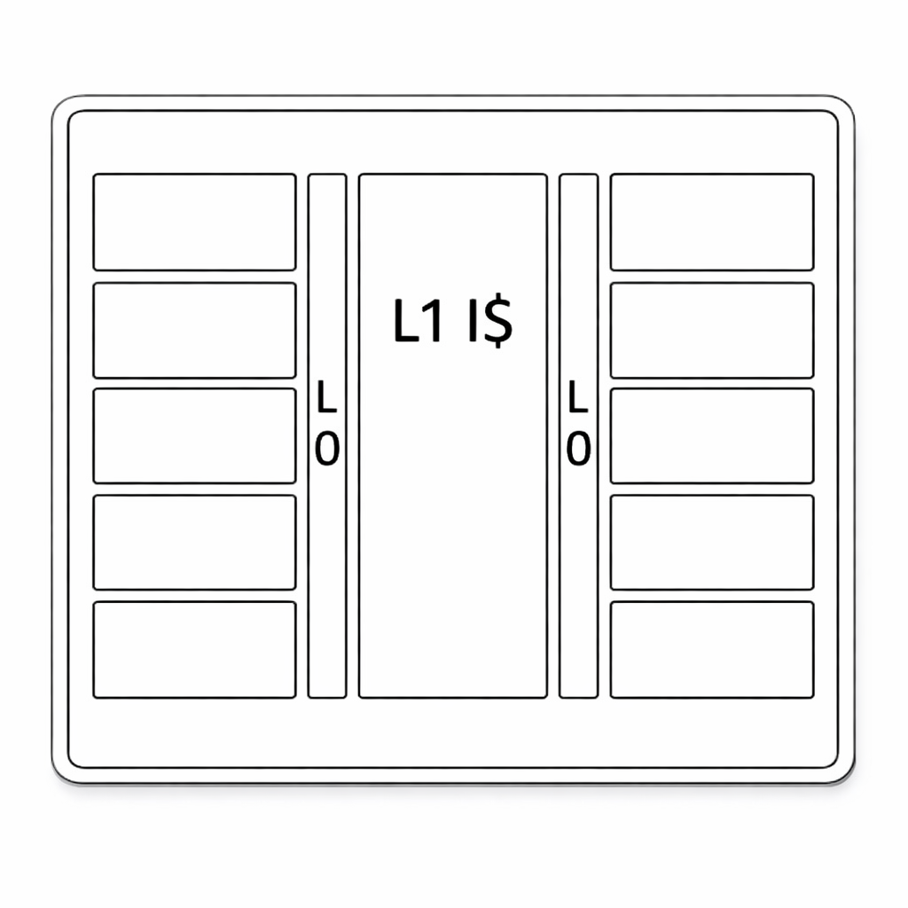
Eight ET-Minions are grouped together in a structure called ET-Neighborhood. The eight ET-Minions in a ET-Neighborhood share some infrastructure within the block: Instruction Caches and input/output buses.
The Instruction Caches are divided into 2 levels, L0 and L1. There are two L0 Instruction Caches, each one shared among a group of four ET-Minions (eight hardware threads). Each L0 Instruction cache has eigh fully-associative entries (so, on average, there is one entry per hardware thread). Both L0 Instruction Caches are then serviced from a local 32KB shared L1 Instruction Cache.
1.3 CPU Subsystem
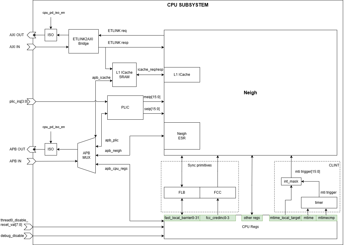
Integrates the ET‑Neighborhood with system‑level infrastructure such as the Platform‑Level Interrupt Controller (PLIC), CPU registers, synchronization primitives (Fast Local Barriers and Credit Counters), and CLINT logic.
2. Programming Model
2.1 ET System Registers (ESR)
ET System Registers (ESR) are memory‑mapped registers: each register occupies a fixed address within this region, and software accesses them using standard load and store instructions. All ESRs are 64 bits in size and aligned to a 64‑bit boundary.
This region is divided into four sub‑regions based on address bits [23:22], referred to as the Protection Bits (PP bits).
The PP bits encode the minimum privilege level required to access a register within that sub‑region:
- 00 — User mode
- 01 — Supervisor mode
- 11 — Machine mode
- 10 — Reserved for microarchitectural messages (e.g., reduce messages, debug accesses) and will always trap as an access fault
2.1.1 Privilege Rules
The PP bits specify the minimum privilege required:
- M‑mode software may access ESRs in PP = 00, 01, and 11 (but not PP = 10).
- S‑mode software may access ESRs in PP = 00 and 01.
- U‑mode software may access ESRs only in PP = 00.
Accesses from a privilege mode that does not meet the minimum PP requirement will raise an Access Fault exception.
2.1.2 Invalid or Non‑Existent ESR Accesses
If software with sufficient privilege accesses an address that does not correspond to an implemented ESR, the access will raise a local Bus Error interrupt.
Because the PP bits are part of the ESR address, each ESR exists in exactly one PP sub‑region. Attempting to access the same register offset in a different PP sub‑region is treated as an access to a non‑existent ESR and will also raise a Bus Error interrupt.
2.2 Register File changes
The integer register file remains unchanged from RV64I. The floating‑point registers (f0–f31) are widened to 256 bits (FLEN = 256). A new set of mask registers (m0–m7), each 8 bits in size, is added to support predicated SIMD execution.
Scalar floating‑point operations (i.e., RV64F instructions) operate only on the low 32 bits of each floating‑point register. Bits 32 through FLEN‑1 are forced to zero as part of the operation.
A new U‑mode CSR, GSC_PROGRESS, is introduced to track the number of elements processed during gather or scatter operations.
2.3 ET-Minion SIMD
As mentioned above, the ET-Minion SIMD extension introduces a set of architectural enhancements aimed at accelerating packed floating‑point and integer workloads. The extension provides eight mask registers (m0–m7), each 8 bits wide, together with basic mask‑manipulation operations. The floating‑point register file is widened to 256 bits, enabling each register to hold eight float32 or eight int32/uint32 elements.
A new class of packed‑single (ps) instructions interprets the widened floating‑point registers as vectors of eight float32 values. All ps operations execute under the control of the m0 mask.
Packed‑integer (pi) instructions operate on the same widened registers but interpret them as eight int32 or uint32 elements. As with the ps subset, all pi instructions execute under the control of the m0 mask.
Finally, the extension provides a group of tensor-oriented pseudo-instructions, implemented via CSR accesses, to efficiently multiply and accumulate float16 and int8 tensors. TensorFMA reads matrices A and B from the L1 scratchpad or memory and accumulates into the floating‑point or TenC register file, operating on 2D tiles in a fixed layout. TensorLoad and TensorStore provide compatible memory transfers for these layouts.
The extension also provides pseudo-instructions to control out‑of‑bounds handling and 2D convolution geometry, and to coordinate reductions across Minions. Cooperative TensorLoad and TensorStore variants are also available, which help coalesce accesses aiming for a better balance of performance and power efficiency.
2.4 Floating‑Point Denormal Handling
Minion does not implement full IEEE‑754 denormal support. All denormalized inputs are treated as zero, and any denormalized results are flushed to zero before being written back.
A sticky InputDenorm flag is added to the machine state. This flag is set whenever a denormalized input operand is flushed to zero during a floating‑point operation. Software may read the flag through either fcsr[31] or fflags[31], and may clear it by writing to either CSR.
2.5 Performance Monitoring Unit (PMU)
The standard minstret and mcycle CSRs, and by extension their user-mode aliases instret and cycle, always return 0.
Counters are implemented in a shared PMU unit covering 8 ET-Minion cores per ET-Neighborhood. The PMU must be explicitly enabled via an ESR write before it counts anything.
The PMU provides 6 programmable counters per HART group. Access is via mhpmcounter3–mhpmcounter8 and event selectors mhpmevent3–mhpmevent8.
The hardware implements only twelve programmable counters: six shared by all even‑numbered HARTs in a ET-Neighborhood and six shared by all odd‑numbered HARTs, so each HART sees only mhpmcounter3–mhpmcounter8.
Other registers like mcycle, minstret, and mhpmcounter9–mhpmcounter31 are hard‑wired to 0.
Counters mhpmcounter3–mhpmcounter6 can count ET-Minion‑related events: the same counter is shared among all HARTs that see it, and the counter accumulates the union of all events configured by any of those HARTs via mhpmevent3–mhpmevent6.
Regardless of whether a HART has configured an event or not, all even‑numbered HARTs in a ET-Neighborhood will read the same value from mhpmcounter3–mhpmcounter6, and all odd‑numbered HARTs in a ET-Neighborhood will read the same value, though different from the even‑numbered HARTs in a ET-Neighborhood, when they read mhpmcounter3–mhpmcounter6. It is the responsibility of the programmer to configure appropriate events into mhpmevent3–mhpmevent6 across the HARTs that share mhpmcounter3–mhpmcounter6 such that the union of events makes sense.
NOTE: For example, if HART 0 and HART 2 both set mhpmevent3 to RETIRED_INST0, then mhpmcounter3 of both HARTs will report the sum of the instructions retired in both HARTs. Similarly, if HART 1 sets mhpmevent4 to RETIRED_INST1 and HART 3 sets mhpmevent4 to CYCLES, then mhpmcounter4 will be incremented on every cycle that HART 1 is executing and whenever HART 3 retires an instruction.
Counters mhpmcounter7–mhpmcounter8 count ET-Neighborhood‑related events; when multiple HARTs configure different events, the counter follows the event programmed by the HART with the lower mhartid (up to 32 ET-Neighborhood events). All even‑numbered HARTs in a ET-Neighborhood read the same value for mhpmcounter3–mhpmcounter6, and all odd‑numbered HARTs read matching but distinct values; the programmer must ensure the set of configured events per shared counter forms a sensible union.
2.6 Privileged Architecture Deviations
ET-Minion implements a variant of the RISC-V Machine and Supervisor ISA v1.11 with the following Erbium-specific deviations that every programmer must be aware of.
satp CSR:
- The satp CSR is shared between both HARTs of a given ET-Minion core. Both threads always operate under the same address space configuration.
WFI Behavior:
- Executing WFI in U-mode always causes an illegal instruction exception.
- When MSTATUS.TW = 1, executing WFI in S-mode also always causes an illegal instruction exception.
2.7 Exceptions and Interrupts
The ET-Minion implements mcause and scause following the RISC-V privileged spec. The MSB indicates an interrupt; remaining bits indicate the cause code.
Standard Interrupts (Interrupt bit = 1):
| Code | Name | Description |
|---|---|---|
| 0 | USI | User software interrupt |
| 1 | SSI | Supervisor software interrupt |
| 3 | MSI | Machine software interrupt |
| 4 | UTI | User timer interrupt |
| 5 | STI | Supervisor timer interrupt |
| 7 | MTI | Machine timer interrupt |
| 8 | UEI | User external interrupt |
| 9 | SEI | Supervisor external interrupt |
| 11 | MEI | Machine external interrupt |
| 16 | MBAD_RED | Bad IPI redirect interrupt (RW) |
| 19 | MIECO | I-cache ECC counter overflow (RO; clear via I-cache ESRs) |
| 23 | BUS_ERROR | Bus error interrupt (RW) |
Standard Exceptions (Interrupt bit = 0):
| Code | Description |
|---|---|
| 0 | Instruction address misaligned |
| 1 | Instruction access fault |
| 2 | Illegal instruction |
| 3 | Breakpoint |
| 4 | Load address misaligned |
| 5 | Load access fault |
| 6 | Store/AMO address misaligned |
| 7 | Store/AMO access fault |
| 8 | Environment call from U-mode |
| 9 | Environment call from S-mode |
| 11 | Environment call from M-mode |
| 12 | Instruction page fault |
| 13 | Load page fault |
| 15 | Store/AMO page fault |
| 25 | Instruction bus error (ET-specific) |
| 26 | Instruction ECC error (ET-specific) |
| 27 | Load split-page fault (ET-specific) |
| 28 | Store split-page fault (ET-specific) |
| 30 | M-code emulation (ET-specific) |
If multiple exceptions and/or interrupts occur at the same time, the decreasing priority order of the following table indicates which trap is taken and reported in mcause/scause:
| Priority | Exception Code | Description |
|---|---|---|
| 1 | — | Interrupts (see discussion below for detailed priority) |
| 2 | 3 | Instruction address breakpoint |
| 3 | 12 | Instruction page fault |
| 4 | 1 | Instruction access fault |
| 4 | 25 | Instruction bus error |
| 4 | 26 | Instruction ECC error |
| 5 | 2 | Illegal instruction (true illegal opcode) |
| 5 | 0 | Instruction address misaligned |
| 5 | 8, 9, 11 | Environment call |
| 5 | 3 | Environment break |
| 5 | 3 | Load/Store/AMO address breakpoint |
| 6 | 30 | M‑code emulation |
| 7 | 2 | Illegal instruction (unknown CSR, permission errors, disabled units, etc.) |
| 8 | 6 | Store/AMO address misaligned |
| 8 | 4 | Load address misaligned |
| 9 | 28 | Store split‑page fault |
| 9 | 27 | Load split‑page fault |
| 10 | 15 | Store/AMO page fault |
| 10 | 13 | Load page fault |
| 11 | 7 | Store/AMO access fault |
| 11 | 5 | Load access fault |
2.8 Synchronization primitives
The Fast Synchronization extension provides mechanisms for coordination among operating ET‑Minions, centered on two facilities: Fast Local Barriers (FLB) and Fast Credit Counters (FCC). These are exposed via both CSRs and memory‑mapped ESRs in the CPU register address space.
2.8.1 Fast Local Barriers
The Fast Local Barrier (FLB) extension offers fast barrier synchronization across ET‑Minions within an ET‑Neighborhood. Multiple barrier counters are implemented as memory‑mapped read‑write registers accessible from user mode. The flb CSR atomically increments a barrier counter and compares its value against a threshold:
- To implement an N‑HART barrier, one HART first clears the barrier counter via the ESR interface, then each HART uses
flbto increment the counter and test whether it is the last to reach the threshold. - The HART is not stalled; the mechanism only signals whether it is the last participant.
Access to these barrier counters does not block execution; they provide lightweight, software‑visible barrier coordination.
2.8.2 Fast Credit Counters
The Fast Credit Counter (FCC) extension provides a fast credit mechanism for coordinating ET‑Minions. Each HART is extended with two local credit counters exposed via the fcc and fccnb CSRs (four counters per ET‑Minion core). One HART can increment another HART’s credit counter by writing to the corresponding CREDINC0–CREDINC3 memory‑mapped registers.
- The
fccCSR consumes credits and can stall the issuing HART until sufficient credits are available. - The
fccnbCSR non‑blockingly reads the current value of the HART’s own credit counters.
Credits can be used directly for producer/consumer synchronization or combined with FLB to implement barriers:
- Initialize by clearing one credit counter on each participating HART and zeroing a fast local barrier.
- When reaching the barrier, each HART uses
flbto test whether it is the last to arrive. - If not last, the HART uses
fccto wait for a credit; if last, it distributes credits via theCREDINCxregisters to all waiting HARTs.
2.9 Core Local Interrupt (CLINT)
The CPU subsystem provides a 64‑bit timer (mtime) that increments every 100 ns (10 MHz) and overflows after ~64,000 years. It is driven from a 200 MHz reference clock via a programmable prescaler configured through time_config; alternatively, it can use an internal ring oscillator for approximate timing.
Timer interrupts are based on mtimecmp: when mtimecmp > mtime, a timer interrupt is asserted and de‑asserted when the condition no longer holds. The timer interrupt is globally broadcast, and software selects which HARTs receive it via mtime_local_target and mie.
Local‑HART interrupts can be generated or cleared directly using the mipi_trigger and mipi_clear registers.
3 ISA changes (Erbium)
Erbium changes the topology compared to ET‑SoC-1, resulting in the following ISA‑level modifications. All supported features remain available except where explicitly removed.
-
ET Atomic extension: Global and local variants now affect the same level of the memory hierarchy, unlike ET‑SoC-1.
-
TensorSend / TensorReceive: These instructions will not be performed and will set
tensor_error[9]if the Receiver/Sender ET‑Minion ID is outside the range0..7. -
TensorReduce / TensorBroadcast: These instructions will not be performed and will set
tensor_error[9]if the tree depth is outside the range0..2. -
Removed instructions:
-
TensorLoadL2Scpis not supported and will raise an illegal instruction exception. -
Deprecated features from ET‑SoC-1:
- The Messaging Extension has been removed.
- The M‑mode Virtual Memory extension has been removed.
- The GFX extensions are still present, except that
frcp_fix.rast,fcvt.ps.rast, andfcvt.rast.pshave been removed and will raise an illegal instruction exception.
4. Erbium Memory
4.1 Memory Map
The Erbium platform uses a 32‑bit physical address which defines a 4 GB address space organized into different regions, as shown in the table below:
| Region name | From | To | From (hex) | To (hex) | Size |
|---|---|---|---|---|---|
| System registers | 32MB | 32MB+4K | 0x0200_0000 | 0x0200_0FFF | 4K |
| MRAM registers | 32MB+4K | 32MB+8K | 0x0200_1000 | 0x0200_1FFF | 4K |
| I2C registers | 32MB+8K | 32MB+12K | 0x0200_2000 | 0x0200_2FFF | 4K |
| QSPI registers | 32MB+12K | 32MB+16K | 0x0200_3000 | 0x0200_3FFF | 4K |
| UART registers | 32MB+16K | 32MB+20K | 0x0200_4000 | 0x0200_4FFF | 4K |
| Bootrom | 32MB+32K | 32MB+40K | 0x0200_8000 | 0x0200_9FFF | 8K |
| SRAM | 32MB+48K | 32MB+52K | 0x0200_C000 | 0x0200_CFFF | 4K |
| xSPI registers | 32MB+60K | 32MB+64K | 0x0200_F000 | 0x0200_FFFF | 4K |
| MRAM | 1G | 2G | 0x4000_0000 | 0x7FFF_FFFF | 1G |
| CPU subsystem | 2G | 2.5G | 0x8000_0000 | 0x9FFF_FFFF | 0.5G |
| PLIC | 2.5G | 2.5G+64M | 0xA000_0000 | 0xA3FF_FFFF | 64M |
| NIC config | 3G+992M | 3G+992M+88K | 0xFE00_0000 | 0xFE01_5FFF | 88K |
As per the RISC‑V spec, if a HART attempts to access a region of memory where it does not have permissions for the type of access performed, or attempts to access a reserved region of memory, then an Access fault exception is generated. If attempts to access a region which is not reserved, but is vacant, a Bus error interrupt will occur. This interrupt is generally fatal/unrecoverable, as subsequent instructions may have been executed.
4.2 Physical Memory Attributes
Each ET-Minion core has a local PMA checker that validates all transactions. This PMA checker is controlled by the ET-Neighborhood mprot ESR, hence all ET-Minions in the ET-Neighborhood will see the same access checks.
| Region name | Cached | Priv | Read | Write | Exec |
|---|---|---|---|---|---|
| System registers | No | M/S | Yes³ | Yes³ | No |
| MRAM registers | No | M | Yes² | Yes² | No |
| I2C registers | No | M/S | Yes³ | Yes³ | No |
| QSPI registers | No | M/S | Yes³ | Yes³ | No |
| UART registers | No | M/S | Yes³ | Yes³ | No |
| Bootrom | Yes | M/S/U | Yes | No | Yes |
| SRAM | Yes | M/S/U | Yes | Yes | Yes |
| xSPI registers | No | M | Yes² | Yes² | No |
| NIC config | No | M | Yes⁴ | Yes⁴ | No |
| MRAM | Yes | M/S/U | Yes⁵ | Yes⁵ | Yes⁵ |
| CPU subsystem | No | D/M/S/U | Yes¹ | Yes¹ | No |
| PLIC | No | M/S | Yes⁴ | Yes⁴ | No |
¹ Access permitted only when all of the following conditions are met: - Hart’s execution mode ≥ ESR privilege mode - Address maps to an existing ESR register (64‑bit aligned) - Read/write access is from a 64‑wide load or store - Instruction is not an AMO, TensorOp, or CacheOp
² Access permitted only when all of the following conditions are met: - Read/write access is 64‑bit aligned - Read/write access is from a 64‑wide load or store - Instruction is not an AMO, TensorOp, or CacheOp
³ Access permitted only when all of the following conditions are met: - Read/write access is 64‑bit aligned - Read/write access is from a 32‑wide load or store - Instruction is not an AMO, TensorOp, or CacheOp
⁴ Access permitted only when all of the following conditions are met: - Read/write access is 32‑bit aligned - Read/write access is from a 32‑wide load or store - Instruction is not an AMO, TensorOp, or CacheOp
⁵ Accesses above the installed MRAM generate a Bus error interrupt.
If access is not permitted by the PMA, the access is not performed and an Access fault exception is generated. The PMAs enforce only the coarse‑grain access rules defined in the preceding table. Passing a PMA check does not guarantee that the access is valid.
A load or store may still be illegal even if the PMA allows the address. This occurs when the target address:
- Does not correspond to any implemented device, device register, or memory location, or
- Corresponds to a device that rejects the access due to alignment, size, or access‑type constraints.
In these cases, a Bus Error interrupt will be raised.
There are also restrictions regarding the type of operation that can be performed at every region as summarized in the table below:
| Region name | RISC-V | AMO | TENSOR | CACHEOP |
|---|---|---|---|---|
| System registers | Yes | No | No | No |
| MRAM registers | Yes | No | No | No |
| I2C registers | Yes | No | No | No |
| QSPI registers | Yes | No | No | No |
| UART registers | Yes | No | No | No |
| Bootrom | Yes | No | No | No |
| SRAM | Yes | No | Yes | Yes |
| xSPI registers | Yes | No | No | No |
| NIC config | Yes | No | No | No |
| MRAM | Yes | Yes | Yes | Yes |
| CPU subsystem | Yes | No | No | No |
| PLIC | Yes | No | No | No |
4.3 Physical Memory Protection (PMP)
The PMP mechanism provides a basic security functionality by defining Machine and Supervisor privilege level subregions inside the MRAM region.
| Address Range | Privilege Access | Description |
|---|---|---|
0x00_0000 → mmode_end |
M‑mode only | Machine‑only region |
mmode_end → smode_end |
M/S‑mode only | Machine + Supervisor region |
smode_end → 0xFF_FFFF |
M/S/U‑mode | Full access region (Machine, Supervisor, User) |
The mechanism can be enabled in the mprot ESR, and the size of the subregions is also configured in the same register.
If disabled, access to the entire MRAM region is allowed for all privilege levels.
When the PMP is enabled:
- mmode_end = 4KB * (2^mprot[mmode_size])
- smode_end = 4KB * (2^mprot[smode_size])
Note that the S-mode region maximum size is limited by the size of the M-mode region. If the size of the S-mode region is 0 or less, it means that the S-mode region does not exist.
Access to the subregions with insufficient privilege level will cause an Access Fault Exception in the ET-Minion PMA.