Power Reset & Clock Management.
Clock and reset signals.
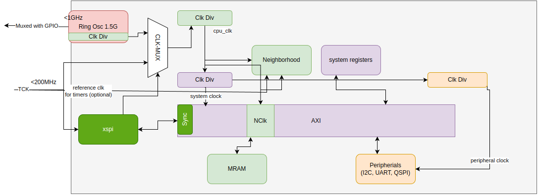
System Clocks
The Device has two clock sources
| Clock | Source | Notes |
|---|---|---|
| TCK | Pin | XSPI Clock Max 200 Mhz. |
| OSC_CLK | Ring Oscillator | Internal Clock Max 1GHz +- 500 MHz |
The OSC_CLK goes through a series of clock Dividers to generate 3 clocks:
- CPU Clock,
- System Clock
- Peripheral Clock
| Clock | Connected IP |
|---|---|
| CPU Clock | Neighborhood, MRAM, MRAM Registers, CPU Registers |
| System Clock | aon logic, PRCM, system reg, BOOTROM, SRAM |
| Peripheral Clock | UARt, I2C, QSPI |
| XSPI CLK | XSPI |
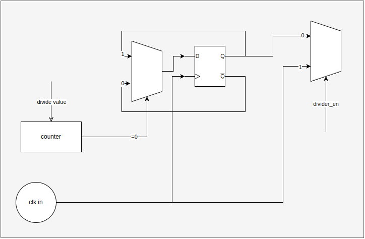
OSC Clock
- This is a high speed clock generated internally from a ring oscillator.
- The raw ring oscillator(RO) frequency is process dependent and can vary by a few hundred MHz from the designed frequency.
- The first level clock divider is programmed to divide the output of the RO by 32 resulting in a <31 MHz boot clock.
- The tester measures the RO frequency, and process variation and writes it to the OTP. This is used to
- Trim the RO to generate a 1GHz clock.
- Program the clock divider to provide the required highspeed CPU Clock.
- Clock dividers can be reprogrammed later as per the system load.
- A second clock divider divides the
high speed cpu clockto generate thesystem clock - Serial protocols require a clock programmed to N times the required baud rate. The Peripheral clock is used as this sampling clock.
xSPI Clock
- This is an external clock with frequency upto 200MHz.
- If required a bit in the xspi register can be written to, to make this the system clock.
CPU Subsystem External Resets
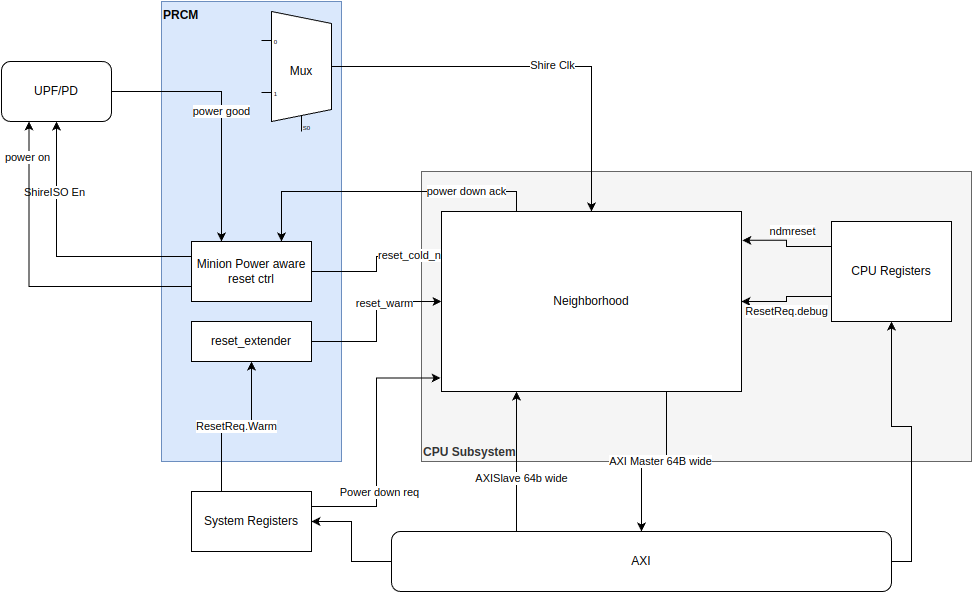
| Reset | Description | Register Programming |
|---|---|---|
| reset_cold | Full Power on reset | From PRCM (POR,soft_reset, brownout) |
| reset_warm | Retains state: Does not reset ESR, VC FIFOs etc. | SoftReset.cpu_warm_reset = 0 |
Reset Sequencing
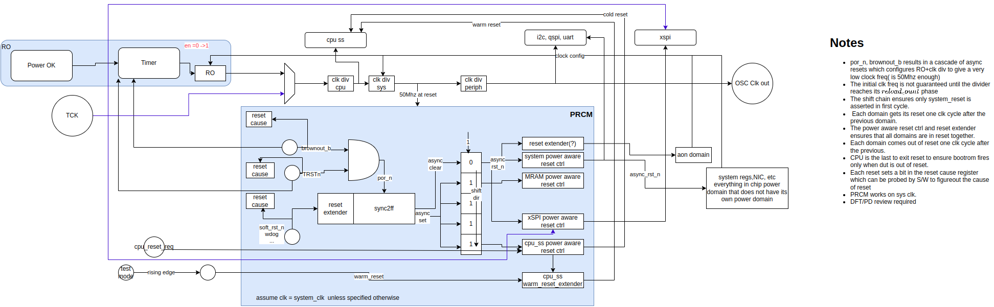
At power on the Ring oscillator and clock dividers have unknown configuration. After reset is applied
- The ring oscillator immediately switched to the default configuration (clock divider enabled, slowest speed).
- Each clock divider latches its configuration(div by 32) only after its internal counter reaches the reload phase.
- The first reset extender ensures that the device remains in reset state until the system divider reloads.
- Power on reset asynchronously resets system registers and xspi ensuring that the correct configuration reaches the ring oscillator, clock dividers and tck/osc_clk mux.
- A Shift register sequences the reset to other modules one by one ensuring that all modules do not enter the reset stage at the same time resulting in a large power drop.
- The reset extender of the power aware reset module ensures that all modules remain in reset for atleast a few common cycles.
- Cpu_system is the last entity to be brought out of reset to ensure that it does not start accessing memory regions that are still in reset.
- At this point cpu subsystem can start programming the ring oscillator and clock dividers to speed up the clock.
Power Domains.
The device contains the following power domains. * Always On. * System Domain. * CPU Subsystem Domain. * Per Minion Power Domain. * MRAM Digital Domain * Each Memory (Bootrom, SRAM and MRAM) has its own power domains. * Each powerdomain is controlled via a power switch. * At Boot every Digital Domain powerswitch is turned on. * The boot routine will check the OTP register for domains that need to be powered down after boot and write to the corresponding system_registers.PowerDownReq bits.
Valid Power State
Simple Power States
| State | Sys PS | MRAM Digital PS | MRAM PS | cpu subsystem PS | ROM/ SRAM PS | minion PS[7:0] | Notes |
|---|---|---|---|---|---|---|---|
| All On | On | On | On | On | On | On | |
| System Off | Off | Off | Off | Off | Off | Off | Extreme low power. Toggle TMS to wake the device |
| CPU Off | On | X | X | Off | X | Off | |
| MRAM Off | On | Off | Off | X | X | X | |
| 1-8 Minions Off | On | X | X | On | On | On/Off | |
| Controlling PowerDomainReq register | system poweroff | mram pd | mram dsleep en | cpu pd | sram pd | minion pd_[0-7] |
Note: * X: Dont care. The domain is usually on. But can be off if a complex Power State is used. * Other than the system off state all other power switches can be turned on by clearing the corresponding pd_req bit. * Complex Power States are: * CPU OFF + MRAM OFF * Minion_x OFF + MRAM OFF
Power State Controller FSM.
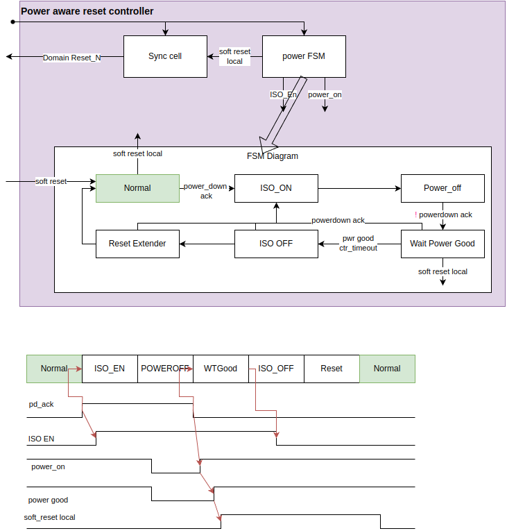
- At boot the FSM is in normal state.
- Writing to pd_req initiates the power down sequence.
- The corresponding domain is informed about the request.
- The domain completes the current outstanding transaction and frees up the system bus and goes into a halt state.
- Domain generates the PD ack signal.
- PD ack signal triggers the Power State Controller which executes the following state changes:
- ISO_EN State: drives the isolation enable signal to the isolation cells placed on the output wires of the power domain.
- POWEROFF State: turns off the power switch and remains in this state until pd req goes low, This can be due to:
- Toggling of TMS signal in case of system power off
- Clearing the corresponding PD Register bit.
- When the pd req goes low this state turns on the power switch and transitions to WTGood State.
- WTGOOD State: It takes some time to ramp up the voltage from 0 to VDD. In this state:
- A counter is initialized with the system_registers.PowerGood.counter register value and counts down to zero.
- State changes to ISO_OFF when the counter is zero.
- soft_reset_req is asserted and stays asserted until we enter the NORMAL state.
- ISO_OFF: the isolation enable signal to the isolation cells is deasserted.
- Note: It is expected the reset values of the domain output signals do not initiate or accept any transaction.
- RESET: We stay in this state for the number of cycles required to propagate the reset to all sub modules in the power domain.
- NORMAL: Normal operation resumes.